![]()
![]()
![]()
![]()
![]()
![]()
|
|||||||||||||||||||||||||||||||||||||||||||||||||||||||||||||||||||||
|
|||||
|
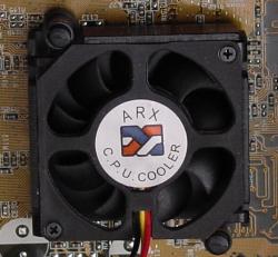
LayoutThe ASUS A7V133 measures 24.5 by 30.6 cm. Giving it a preliminary once-over, one sees that it bears the 462-pin Socket A, 3 DIMM slots for 1.5GB or 6 banks of either PC133 or VC133 SDRAM, 4 IDE ports, two of which are controlled by the Promise PDC20265R ATA100/RAID controller, one AGP Pro slot, 5 PCI and one AMR. The chipset is comprised of VIA's VT8363A north bridge and VT82C686B (or simply "686B") south bridge. The important thing about the chipset is that while on earlier KT133 boards you could run a 133MHz Athlon at 133, but it still wasn't "official" and amounted to an overclock. With the KT133A, 133MHz is the baseline FSB, and you can move up from there, even with Duron processors, which are actually only designed to run at 100! As with the predecessor KT133, this northbridge runs very hot. On the A7V133, ASUS has followed the lead of other companies and included an active cooling fan on this north bridge instead of a typical passive heatsink.
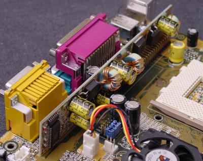
The configuration of the peripheral slots is somewhat bewildering: AGP Pro cards are still considered super high-end. AMR is considered low-end. The presence of both give the board a somewhat schizophrenic quality. With current boards, the AMR slot has been moved from its former location between the AGP and PCI 1 to the very south edge below PCI 5. This is the place where we had been seeing CNR slots on Intel boards, and it is easy to mistake one for the other. But make no mistake about it; this is an AMR slot, which you are just about as likely to use as as AGP Pro card. Then we come to the most immediately noticeable part of the A7V133, the piece of PCB-cum-riser held at a perpendicular angle to the board itself. This is the location of several transistors, capacitors, and inductor coils, and ASUS has been using this solution for all its Socket A motherboards, starting with the original A7V. Presumably, they decided upon the riser rather than crowd the board with all the power-converting components needed by the voltage-hungry Thunderbirds.
I had heard that this riser can get quite hot, so I attached an extra thermal sensor to it (the A7V133 provides an extra header, labeled JTPWR, for such sensors) and tracked its temperature during the course of my tests. It did in fact reach temperatures of 43 degrees C at times. On the south side of the board, to the east between PCI 4 and 5 is ASUS' own AS99127F ASIC chip for hardware monitoring. ASUS chose this solution instead of the VIA hardware monitoring usually seen with VIA chipset motherboards, and it can be used in conjunction with the ASUS PC Probe software included on the CD to give real-time voltage, temperature, and fan-speed reports. A little green light tells you when the board is powered on. Though useful, it is tucked away between the AGP slot and PCI 1, and is somewhat difficult to see with all components installed. There are 2 USB ports and a header for two more; an extra connector set is included with the board.
|