![]()
![]()
![]()
![]()
![]()
![]()
|
|||||||||||||||||||||||||||||||||||||||||||||||||||||||||||||||||||||
|
|||||
|
Configuration
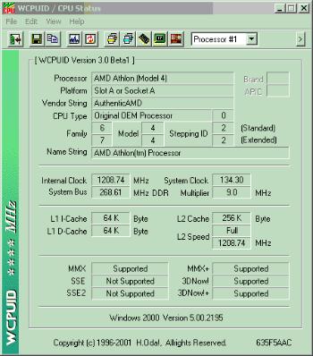
InstallationFor the most part, installation of the board was easy. The space around the CPU was sufficient for my Titan D3 cooler. 126MB of Siemens CAS2 PC133 SDRAM went into DIMM 1, the slot closest to the boards' edge. The DIMM clips in no way interfered with the AGP card. The sound card went in PCI 3, the Western Digital hard drive went in as the master device on the primary native IDE port, and my CD-RW went in as the master on the secondary native IDE port. All the FSB and multiplier DIP switches remained in their default positions (all ON), as this enables the JumperFree BIOS. As I was using a separate sound card, I had to move the set of audio jumpers to disable the onboard sound. For the third and fourth IDE ports (those controlled by the Promise chip), one must also use jumpers to select either ATA/100 or RAID, which I left at ATA/100 for the time being. Also, while the CPU core voltage can be adjusted in the BIOS (assuming that the corresponding jumpers are left in the default positions), the I/O voltage can be adjusted by jumper only. For now, I left these at the default of 3.45v. Plugging in the power supply and booting up, I got to the POST screen with no problem. The memory was correctly counted and the CPU was detected as 1.2GHz. But upon pressing delete to enter the BIOS screen, I discovered a few oddities. First of all, the CPU was detected as 1.2 GHz, true, but the BIOS identified it as having a 100MHz FSB with a 12x multiplier. A little strange, considering that the sole purpose of the KT133A chipset is to provide official 133MHz support. Even if you have no intention of overclocking, you still must set the CPU frequency to “User Define,” in my case changing the FSB to 133 and the multiplier to 9x. To do so, you would have to use a pencil to rebuild the L1 bridges (unless you have an engineering sample with the bridges intact, as I did). Most of you reading this review plan to do so anyway, but it’s a consideration if you had intended to stick to the default speeds. I also noticed that there was no host clock to DRAM clock divider, so if I had wanted to run my Athlon at 133 with the memory at 100, I would have been out of luck.* The second oddity was that the BIOS had not detected my hard drive at all. After shutting down the board and changing around my HDD/CD-RW configuration a few times, I discovered that the problem lay in the primary (blue) native IDE port. If I put the CD-RW on this channel as either master or slave, it was detected with no problem. Also, the secondary (black) native IDE always detected the HDD correctly. However, the HDD simply could not be detected on the primary port, no matter what the configuration, and in the end I had to set it as the master (with the CD-RW as the slave) on the secondary port. These IDE problems are probably limited to this board alone, as they have not been mentioned in the other reviews of the A7V133. If anyone has experienced a similar problem, please e-mail me. Everything else in the BIOS was just as it should be. The default AGP setting was 4x, though Fast Write had to be enabled manually. Under Chip Configuration in the “Advanced” menu, I changed the CAS Latency setting to 2. In the same section, I also made sure that DRAM Bank Interleaving was set to “Auto” rather than “None.” I would have like to see a greater variety of options here, such as a choice between 2-Way and 4-Way as we’ve seen on other boards, as memory tweaks are rapidly becoming the most important aspect of performance optimization. A clean install of Windows 2000 later, as well as VIA 4in1 drivers v2.9, Nvidia Detonator 6.31, and the Promise chip driver (from the ASUS CD) later, and I was ready to go. Note that I did not upgrade the BIOS to the then most recent version 1004, as the ASUS site described it as fixing DIMM detection VIA codec ID errors, neither of which were a problem for me. I proceeded to check WCPUID and found that though I had chosen 133, the system clock was actually running at 134.30, giving me a CPU clock of 1.208GHz and change. ASUS’ motherboard monitor reported the CPU temperature at 46 degrees C, which I felt comfortable with for the time being.
*NOTE: Since the original posting of this review, it has come to my attention that 12x100 is the default boot for an engineering sample CPU with connected L1 bridges. I have not had the opportunity to test this board with a mass-production sample Athlon, but a few readers have informed me that the A7V133 successfully detected their CPUs with 9x133 as the default.
|